

")
JTAG Visualizeris an advanced graphical viewer and data management system for PCB schematics and layouts. Visualizer integrates seamlessly with the JTAG Technologies family of boundary-scan products, such as the ProVision application development platform, and accepts PCB data from a variety of CAD, CAM and EDA tools. In design Visualizer provides DfT (design for test) feedback to the user by enabling a graphical view of fault coverage on their design. In manufacture and test Visualizer can be used to highlight faulty nets (short circuits, opens, stuck-ats etc.) in both layout and schematics views.
Use Visualizer for schematics to assess the test coverage/impact of boundary-scan early in the design cycle. Add test coverage data from complementary test systems (functional, ICT, flying probe etc.) and view combined assessment through Visualizer. Use Visualizer for layout in production test systems to highlight data from the boundary-scan diagnostics reporter (BSD). Integrate Visualizer into bespoke test executives with the Active-X version also included.
- Supports PCB layout and schematic views
- Large number of input data sources
- Stand-alone or plug-in to JTAG ProVision
- View and print color-coded fault coverage data early in design cycle
- Most EDA formats from Mentor, Cadence, Altium, Zuken etc., accepted
- CAM formats also accepted for layout data (FabMaster ODB++ etc.)
- Simplifies fault finding in repair and rework
- Imports and displays schematics and layout data from most manufacturers, such as Mentor, Cadence, Altium, Zuken, Valor, etc.
- Link to Vizualizer layout or schematic direct from ProVision netlist explorer, fault coverage examiner, boundary-scan diagnostics reporter and more.
- Use Active-X version to add the power of Visualizer to you own bespoke test executive
- Fully customizable display modes for net colors highlights etc.
- Cross-probing between layout and schematics at component and net levels.
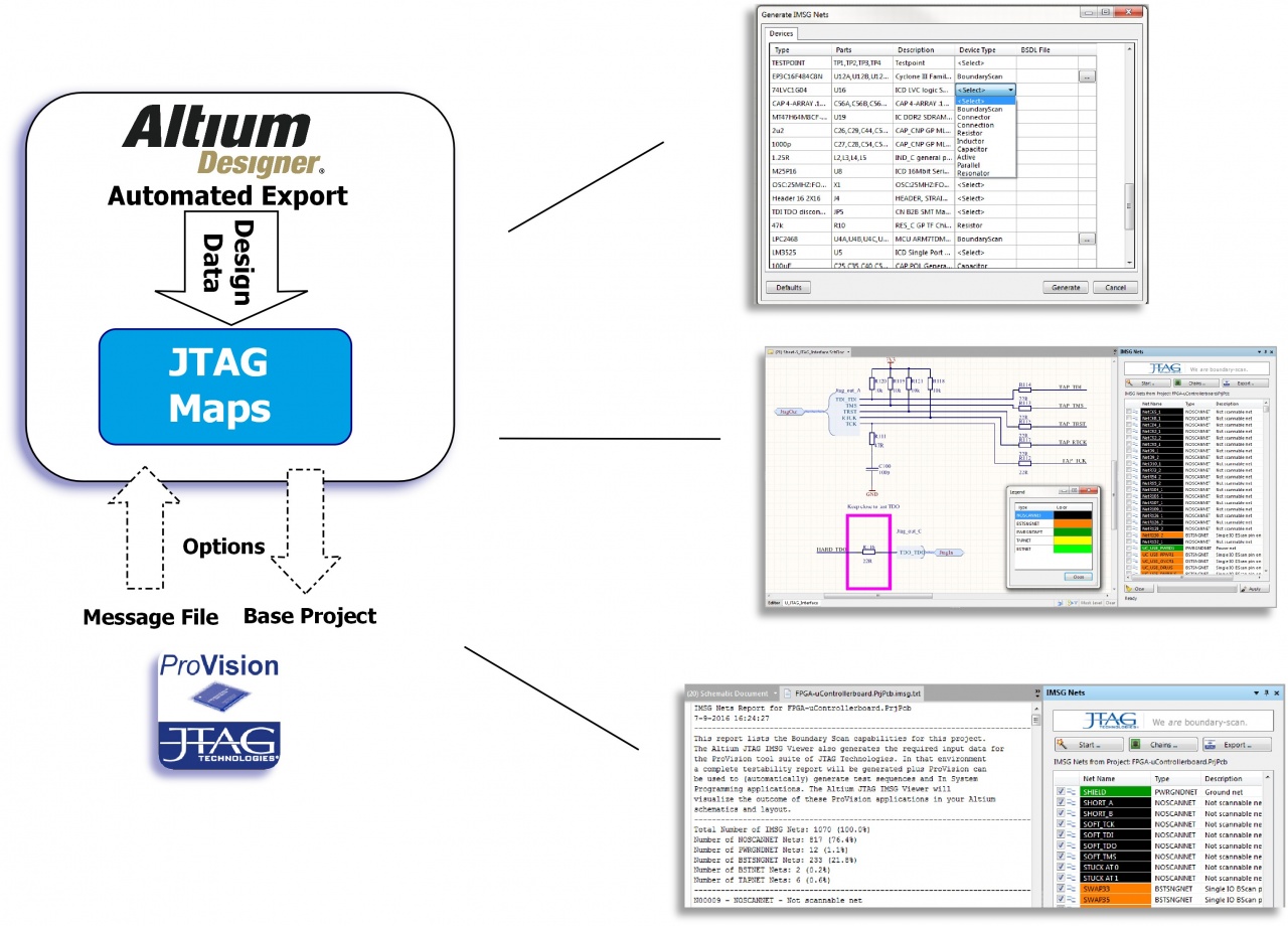
JTAG Maps is an extension to Altium Designer that allows the user/engineer to quickly assess the capabilities of the JTAG devices on their design. Until now engineers could often spend hours highlighting the boundary-scan nets of a design manually to determine fault coverage. Today the free JTAG Maps for Altium application does all this and more, freeing-up valuable time, allowing a more thorough DFT and speeding time to market.
JTAG Maps visualize on schematic and gives coverage reports on three levels. The lowest one bases only on schematic analyses and on identification of on-board B-S infrastructure. It means that connections of TAP port lines like TMS, TCK, TDI, TDO, TRST are detected and highlighted. The higher level uses BSDL device models delivered by semiconductors vendors. These models indicates precisely which pins can be controlled or observed while boundary-scan testing. On the highest level it requires JTAG ProVision. Coverage reports can be exported/imported between JTAG Maps and JTAG ProVision for further analysis. JTAg Maps can visualize such extended reports.
JTAG Maps is the ideal companion tool to Altium Designer for engineers with a responsibility for DFT (Design for Test). JTAG/Boundary-scan is widely acknowledged as the principal method for testing PCB assemblies with a digital content (utilising devices such as FPGAs, CPLDs, Microprocessors, Microcontrollers etc.). JTAG Maps allows a quick and easy view of your design's boundary-scan test potential.
- Rapid display of boundary-scan accessibility
- Aids DFT process
- Speeds product development and reduce time-to-market
Optional Developer Tools - for engineers wishing to apply JTAG/Boundary-scan tests directly onto their design JTAG Technologies can offer two further options:
- JTAG Live for low cost functional testing with boundary-scan
- JTAG ProVision a full-blown automated test program generation and device programming system